 Xtremehardware
La nuova risorsa italiana di hardware e overclock
CPU
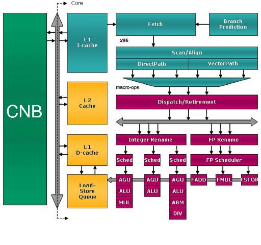
The core architecture of the Llano resumes and improves the one of the "Stars" core, with some improvements visible even from the block diagram.

The green block, contains the North Bridge, the I/O controller for the chip and the RAM controller and is shown in the figure, with label CNB. It will be described later.
The gray BUS that you see on the side of the CNB is the only bus onto which all the core comunicate and on which they are enabled to communicate, in turn, by the NB.
The rest of the diagram includes a core and its caches.
Power Saving Techniques
From the description that follows in subsequent pages, for those who already know the previous Stars architecture, it would seem that not much has changed. Actually in the Llano core has been implemented a wide range of advanced energy saving techniques.

First, the grid that distributes the clock has been completely redesigned and made sparse, ie those branches which were eliminated did not carry the signal to any unit. Then the clock gating was implemented in the various units and with a very high granularity.
The clock gating consists in shutting down clock at parts of a chip to drastically reduce consumption.

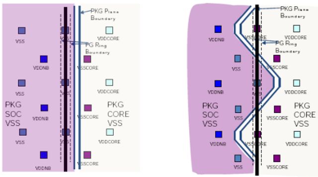
Finally, the CC6 energy-saving state was introduced which consists in removing the physical power to the entire core, through a ring of about one million transistors around each core.
It was estimated by AMD that energy saving is equal to 16% at full load, 36% at idle and over 90% in the CC6 energy saving state, compared to a Stars core, by normalizing the consumption for the clock, for the production process and for the number of transistors.
This means that if the Llano core had been made with the 45nm manufacturing process and had the same number of transistors of a Stars core, it will consume as indicated. It has been estimated also that normalizing the consumption as mentioned above, on average, a Llano core consumes 25% less.
The differences with the Stars core are impressive, especially in the state of maximum energy saving, that does not exist in the core of the old generation, as a core was taken at idle to 800 or 1000 MHz, reducing but not eliminating power consumption. In particular there was no clock and power gating.
All this was possible thanks to the excellent SOI process that has been further improved, but as we can see, with Llano has been achieved even more, thanks to the introduction of these new technologies.
Such techniques on the clock grid, on the clock and power gating have been extended to the North Bridge and the GPU, which also benefits from the transition to the 32nm HKMG SOI gate first process of Global Foundries.

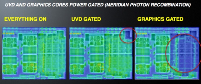
As you can see from the thermal image, the rings of transistors are very effective in reducing heat dissipation. Without them, but only the clock gating, the leakage would remain, being very low in the SOI process, up to 10-20 times less than the competition. But the 32nm HKMG SOI gate first process allows you to use an N-MOS transistor ring, which are able to reduce further the already low leakage by a factor of 10.
Competition instead uses a gate last process, which requires the use of P-MOS transistors, less effective for power gating. Result? The of parts do not almost absorb current, and remain almost at room temperature. A big step forward compared to the Stars core.
Getting more into energy saving operation, we can say that Llano has two separate supply voltages: VDD and VDDNB. On the first line, all the cores are connected, which then are fed by the same voltage. On the second line the remaining units of the chip are connected: the northbridge, the GPU, the UVD block and the GIO block
Apparently it may seem inefficient to connect all cores at the same voltage, because the VDD must be equal to the maximum voltage required by all cores. But the deep clock gating, the deep power gating, the CC6 state for the cores, the lithography process with a very low leakage and the high efficiency of the N-MOS at the core shutdown allow almost zero consumption for the unused cores.
There are actually two types of C6 power state. The CC6 (Core C6) is the maximum energy saving state of a single core, as we have already seen. But if at least one core is active, the VDD voltage and the clock generator can not be turned off, consuming energy. Here comes the second C6 power state, more profound, called PC6 (Package C6), which engages when all the core have gone in the CC6 state. In this case both the supply voltage and the core clock can be switched off, leading to additional savings.
As for the VDDNB, here a single voltage is a compromise to reduce the complexity of the system, but always with very granular clock gating and power gating, energy savings can be substantial.
As for the core, the VDDNB must be set to the maximum voltage required by the powered components. The northbridge has its own P-states, as well as the GPU, with its memory controller, which is one of the most consuming components of the system and that can be turned off independently of the GPU, the UVD and GIO unit (P-State depends on the speed of PCI Express links, 1.0 or 2.0, which requires higher voltage).
As for the GPU, it can be turned off automatically by the hardware, using a programmable timer from the BIOS or graphics driver itself. But as for the cores, clock gating and power gating, combined with the advanced production process, allows optimum power consumption, as seen in the thermal image above.
Other energy-saving techniques implemented, consist of frame buffer data compression, allowing you to transfer less data and therefore save energy and a technique implemented in the mobile version, called adaptive backlight modulation (ABM), which consists in modulating the brightness of the display backlight lamp according to the displayed content, to reduce energy consumption without affecting the images displayed in a visible way.
